


Magnetics Enable Next-Generation Semiconductor Materials and 3D Packaging
As semiconductor designs evolve, the industry is looking beyond silicon to unlock new performance gains. Advanced materials and 3D packaging architectures are reshaping the landscape, enabling higher efficiency, greater power density, and new levels of integration. Here again, magnetics play an essential role in making these breakthroughs possible.
New Materials for Next-Generation Devices
The adoption of gallium nitride (GaN), silicon carbide (SiC), and other compound semiconductors is transforming chipmaking, particularly in power electronics and RF applications. These materials offer advantages in speed, efficiency, and thermal performance, allowing chips to operate in environments where traditional silicon falls short.
Magnetics intersect at several stages:
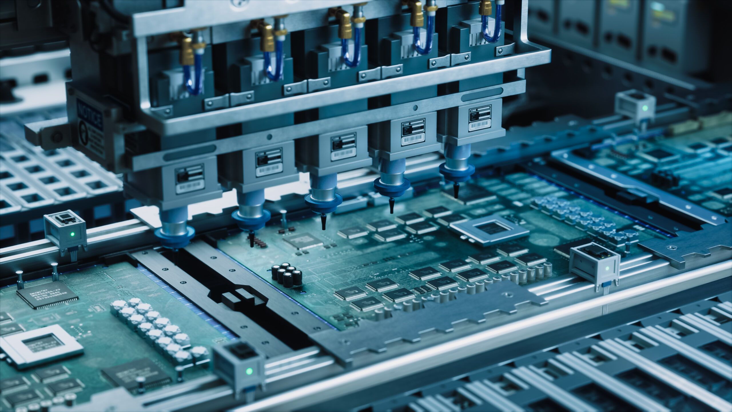
- Ion implantation systems use strong magnetic fields to control particle beams when doping new materials.
- Wafer handling relies on precision magnetic motion to maintain contamination-free environments.
- Magnetic sensing tools help monitor and control uniformity during advanced material processing.
The Rise of 3D Packaging 
As devices shrink and workloads expand, traditional 2D scaling is no longer enough. 3D packaging technologies—such as chiplets, through-silicon vias (TSVs), and heterogeneous integration—stack and connect multiple dies into compact, high-performance systems.
These architectures require precise alignment and bonding at microscopic scales. Magnetic solutions support this by:
- Enabling high-accuracy wafer alignment and positioning.
- Supporting non-contact inspection systems that rely on magnetic sensing for quality control.
- Improving throughput with magnetic actuators in robotic handling during assembly.
Industry Leaders Driving Change
- TSMC – Pioneering 3D packaging with chiplet and TSV integration.
- Intel – Advancing multi-die solutions with Foveros and EMIB technology.
- Amkor Technology – Delivering high-volume manufacturing capabilities for stacked and fan-out packaging.
Permag’s Contribution
Permag™ develops the magnetic systems that make these advanced processes possible. Our solutions include:
- Magnet assemblies for ion implantation in GaN and SiC.
- Custom wafer handling actuators designed for high cleanliness and repeatability.
- Magnetic sensing tools for precise measurement in 3D packaging and inspection.
With expertise spanning Dexter Magnetic Technologies, Electron Energy Corporation, and Magnetic Component Engineering, we provide reliable, application-specific magnetic designs to help fabs and equipment makers embrace the future of materials and packaging.
Looking Ahead
As new materials and packaging architectures push device capabilities beyond silicon, magnetics will remain critical for both precision and scalability. In the next article, we’ll explore how AI, quantum computing, and automation are transforming fabs into smarter, faster, and more adaptive environments.