


How Magnetics Enable Next-Generation Semiconductor Manufacturing
As the semiconductor industry pushes the boundaries of performance and miniaturization, two technologies sit at the heart of next-generation chipmaking: advanced lithography and plasma control. These innovations are reshaping how fabs print smaller, more powerful circuits with fewer defects. Behind both lies a critical enabler—magnetics—delivering the precision, stability, and efficiency needed for success.
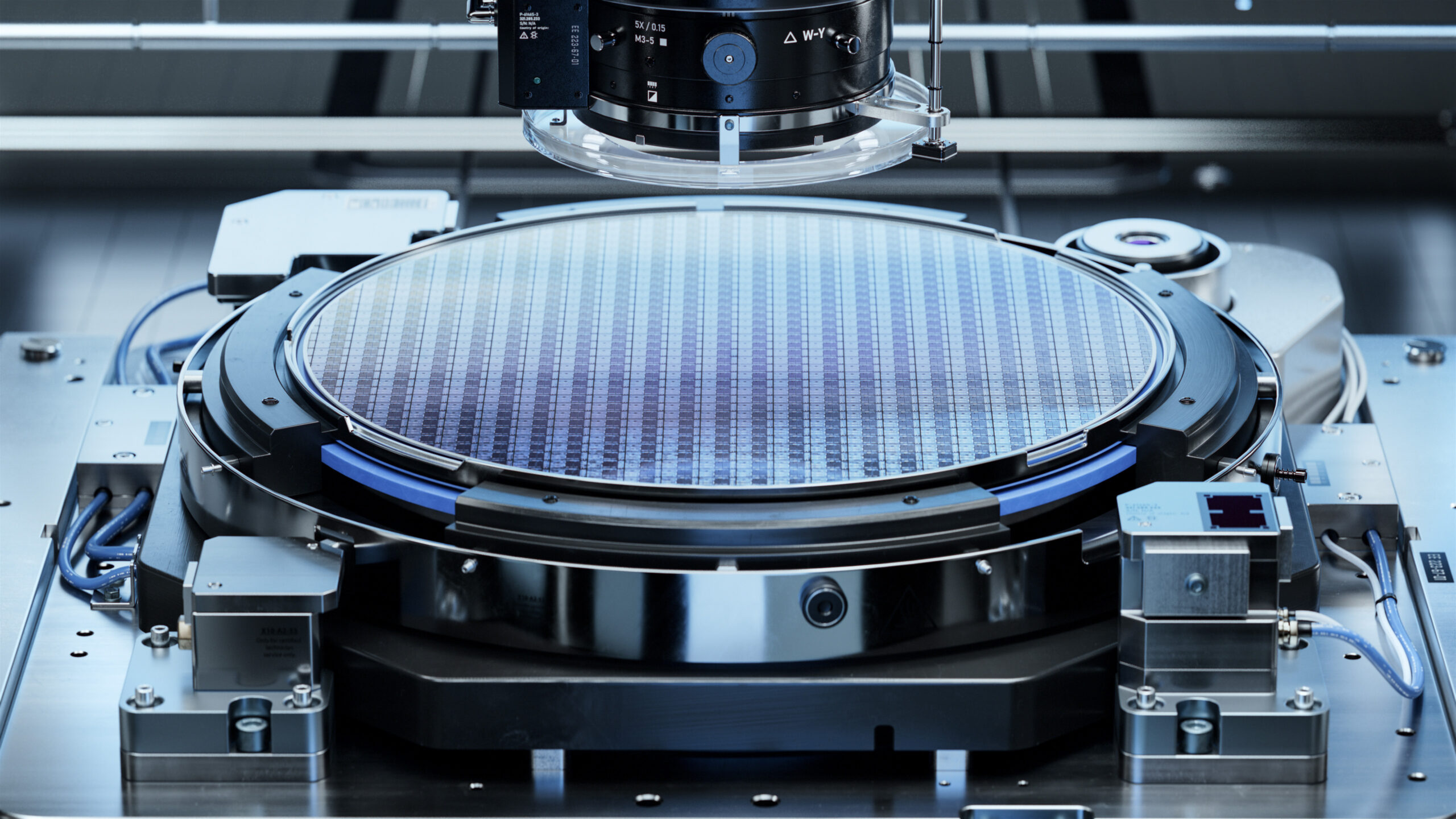
Permag Delivers Magnetics in semiconductor manufacturing
The Rise of Extreme Ultraviolet (EUV) Lithography
Lithography defines the geometry of integrated circuits, and the shift to Extreme Ultraviolet (EUV) light has enabled sub-7nm nodes. EUV tools expose wafers with ultra-short wavelengths, allowing finer patterning than traditional deep ultraviolet systems. Now, development is accelerating toward High-NA EUV, which promises even higher resolution, critical for keeping Moore’s Law alive.
To achieve this level of precision, EUV systems demand flawless motion control. Wafer stages must move with nanometer-level accuracy while maintaining vibration-free stability. This is where magnetic technologies such as linear motors, actuators, and magnetic bearings come into play. By enabling smooth, high-speed motion and reducing friction, magnetics ensure that wafers are precisely aligned during exposure—without introducing the wear and tear associated with traditional mechanical systems.
Plasma Control: The Unsung Hero of Chip Fabrication

Beyond lithography, plasma-based processes drive deposition, etching, and ion implantation—the steps that sculpt modern transistors and interconnects. Plasma uniformity and stability directly impact yield, especially as fabs push to extreme aspect ratios in 3D structures like FinFETs and Gate-All-Around transistors.
Magnetic fields are central to plasma confinement and control. Magnetron sputtering, for example, relies on magnetic fields to trap electrons near a target, increasing ionization and deposition efficiency. In etching and ion implantation systems, permanent magnets and electromagnets help steer plasma precisely where it’s needed, improving process repeatability while minimizing defects.
By advancing plasma control, magnetics not only enhance precision—they also increase throughput and reduce scrap, delivering both technical and economic benefits for semiconductor fabs.
Key Industry Drivers
Leading equipment manufacturers are heavily investing in these areas:
- ASML – Dominating EUV lithography with ongoing innovation in High-NA systems.
- Applied Materials – Developing deposition and etching platforms that integrate magnetic solutions for plasma control.
- Lam Research – Known for etch and plasma-enhanced processes that depend on advanced magnetic confinement.
These companies highlight the industry’s recognition that precision lithography and plasma control are inseparable from advanced magnetic technologies.
Permag’s Role in the Future of Chipmaking
At Permag™, we understand the critical role magnetics play in enabling next-generation semiconductor technologies. Our expertise spans:
- High-performance motors and actuators for wafer stage control.
- Permanent magnets and electromagnets for plasma confinement and deposition systems.
With decades of experience across Dexter Magnetic Technologies, Electron Energy Corporation, and Magnetic Component Engineering, Permag provides the custom magnetic solutions fabs and equipment manufacturers need to push the limits of lithography and plasma processing.
Looking Ahead
This is just the first in our series exploring how magnetics intersect with the future of semiconductor manufacturing. From advanced materials and packaging to AI, robotics, and green manufacturing, each advancement relies on precision magnetic solutions to make innovation possible.
As fabs demand higher efficiency, smaller nodes, and lower defect rates, Permag will remain a trusted partner—helping customers achieve performance at the cutting edge of semiconductor technology.